When Electronics Meets Chemistry: A Conductivity Sensor For Liquid Solutions

Every now and then, my wife asks me to build a gadget that she can use in school for her demos, or for the students labs. This time she asked me for a device able to figure out if a liquid solution has low or high resistivity. Basically, if it is an ionic or covalent solution.
Here is what I put together for her in just a week-end.

Every now and then, my wife asks me to build a gadget that she can use in school for her demos, or for the students labs. This time she asked me for a device able to figure out if a liquid solution has low or high resistivity. Basically, if it is an ionic or covalent solution.

Here is what I put together for her in just a week-end.

It is a simple circuit that turns on an LED if a simple probe is put in contact with an ionic solution with relatively low resistance.

Since it needs to be portable, it is powered with a simple 9V battery.

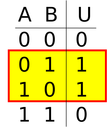
The circuit uses an op-amp configured as a voltage follower. The output is connected to a green LED which lights up if the output goes low.

The non-inverting input is connected to the +9V through a resistor, which I calibrated empirically. Because the non-inverting input is connected to the +9V, the output will also be high and the LED will be off.

However, I can also connect the non-inverting input and the ground of the circuit to the solution through a couple of wires. If the resistance of the solution is low enough, the voltage at the non-inverting input will lean toward ground, making the op-amp output to switch to low which, in turn, will turn on the LED.

Simple enough, don’t you think?

My wife’s students will use this device to check the conductivity of a solution, to determine if the material they put in some distilled water is an ionic or covalent compound. The LED will turn on only with ionic compounds, that will decrease the resistivity of the distilled water.

For this simple device, I designed in OpenSCAD a small box to contain it. Here is the corresponding code:

$fa=0.5;
$fs=0.5;

//body
difference()
{
    cube([52, 23, 70]);
    translate([1, 1, 1]) cube([50, 21, 70]);
    translate([23, 1, -1]) cube([6, 3, 3]);
}

// cap
translate([0, 35, 0]) difference()
{
    cube([55, 26, 30]);
    translate([1, 1, 1]) cube([53.5, 24, 30]);
    translate([(55-14.5)/2, (26.5-9.5)/2, -1]) cube([14.5, 9.5, 4]);
    translate([(55-14.5)/4, 26/2, -1]) cylinder(d=5, h=4);
}

and here is a picture from the OpenSCAD preview window:

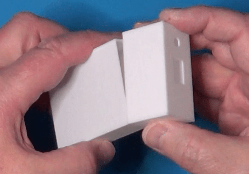
Here, instead, is a picture of the actual case:

Now a picture of the prototype mounted on a breadboard:

Testing of the device requires a small cup of plain water. We submerge the tip of the sensor (the two breaded wires) in to the cup and make sure that the LED stay off. Then we add a pinch of table salt to the water and try again. This time the LED must turn on, to signify that there is an ionic compound mixed in the water.

I mounted the circuit on a half piece of solderable breadboard.

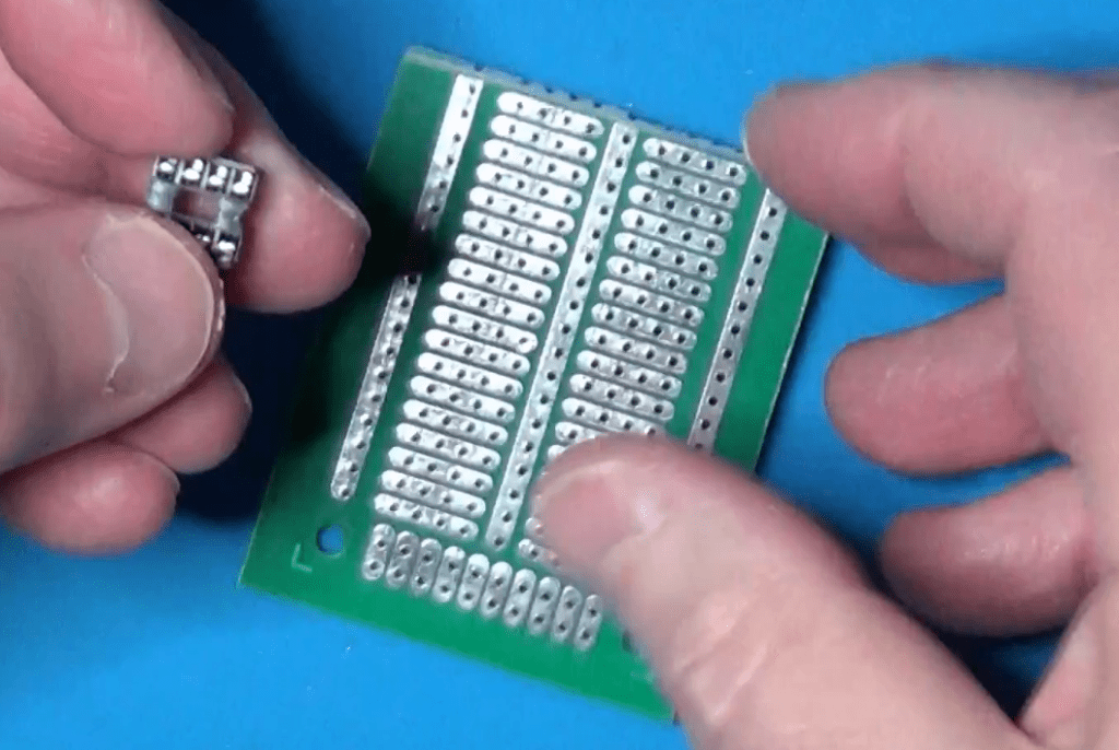
I have chosen to cut the board in half for two reasons:

  1. The circuit is very small and does not require that much space to assemble it. Moreover, being small it will be easier to handle it with a single hand when using it in a chemistry lab.
  2. Using a solderable breadboard rather than a perfboard simplifies the wiring, because it is reduced just to some jumpers to complete the connections already available on the board.

These boards are very easy to find in online stores. I usually by mines on Amazon, but also other stores that sell electronic components have them available. Of course, you are free to use any kind of board you like, be it a simple perfboard, or a solderable breadboard, or a strip-board, or even make your own PCB.

I decided not to use the PCB because of the simplicity of the circuit. With so few components, making a PCB and put the components on it would have not saved me time, nor there was much risk of making mistakes.

Once the circuit on the board was completed, I put it inside the case I made for it, and completed the assembly with the LED and the power switch mounted on the cover. I also decided to use some tape to hold the cover on the case, considering that these little devices will be managed by students, and I don’t want them to easily open it and break it.

As an alternative, I could have used a couple of small screws to hold everything together, but this was something I had to do over a single week-end, so I decided to go through the fastest possible route for the design of the case.

My wife used the device in school right on the next day after I made it. She told me the sensor worked perfectly and her chemistry students enjoyed using it, while experimenting with different compounds to verify their nature.

All in all I am satisfied. I was able to design and build five of these devices in just a week-end, and they were all up to the expectations, of my wife of course.

If you are interested in making this device and would like to see more details on its construction, please click on the following link which will take you to my youtube video with the whole story:

Digital Electronics Fundamentals 4: Universal Gates

There are certain logic basic gates that can be used to reproduce the functionality of any other gate. To do that, these gates need to be able to do inversion in addition to their basic functionality. They are the NAND gate and the NOR gate. In this article, we will examine how that can be achieved.

NAND, NOT, AND

Let’s start with the NAND gate.

NAND gate

If we tale a look at the truth table of such gate, we find that considering only the first and the last row of it, it behaves exactly like a NOT gate.

To make it work, we just need to put together the two inputs of the gate, and it will work as an inverter.

NOT from NAND

Given that, we can easily build an AND gate out of two NAND gates. The first gate provides the NAND function and the second provides a NOT function that converts the NAND into an AND.

AND from NAND

At this point, before showing how to create any other gate from the NAND gate, we have to enounce the De Morgan theorem, which will allow us to manipulate the boolean expressions of the various gates to convert them into a number of NAND gates connected together.

De Morgan Theorem

The theorem states that we can convert a NAND operation into an OR operation, and we can also convert a NOR operation in to an AND operation, according to certain rules. Here is the theorem expressed in boolean algebra:

De Morgan Theorem

If you like to verify that the theorem holds true, just build the truth table for the right side of each equation and compare it with the truth table of the corresponding left side, which are respectively a NOR and a NAND truth table. The tables on the two sides should be identical.

OR from NAND

Let’s see now how we can make an OR gate using a circuit with only NAND gates.

Here is the symbol of the OR gate:

And here is its truth table:

Let’s now write down the boolean expression for the OR gate and let’s apply to it the De Morgan theorem so we can convert everything to AND and NAND.

The one on the right is the boolean expression of the OR gate expressed in terms of NAND gates, and we can convert it in to a digital circuit like this:

OR from NAND

Again, to prove that this circuit really behaves like an OR gate, we can deduct its truth table and compare it with the one of the actual OR gate. If they are identical, this circuit effectively mimics the OR gate. try yourself and, if you have difficulties, please take a look at the companion video on YouTube. The link is at the end of this post.

NOR from NAND

Like we did for the OR gate, we could determine the boolean expression of the NOR gate and find how to build the circuit that mimics it. However, since the NOR gate is essentially the same as the series of the OR gate and the NOT gate, we cna just reuse the previous circuit and add the NOT at its output, as in the following picture:

You can demonstrate the correctness of this circuit by comparing again, its truth table with the one of the NOR gate.

XOR from NAND

To convert the XOR gate in to a combination of NAND gates, we need to start from its truth table:

Now we can write down the boolean expression of the XOR gate by referencing to the lines of the truth table that have an output of one, like we have seen in the previous episode. One we have the XOR boolean expression, we can manipulate it using De Morgan to obtain a form that can be described with NAND gates only:

And, finally, we can draw the digital circuit corresponding to the rightmost part of the above boolean expression:

XOR from NAND

And this is the circuit that mimics the XOR gate using only NAND gates. And guess how we can prove that?

XNOR from NAND

For the XNOR gate, we could just add a NOT at the output of the previous circuit. However, we can use one less NAND gate if we redo the whole procedure we made for the XOR gate.

Here is its truth table:

Here is the derived boolean expression appropriately manipulated:

And here is the corresponding schematic made only of NAND gates:

XNOR from NAND

NOR, NOT, OR

Let’s now talk about the other universal gate: the NOR gate.

NOR gate

Here is its truth table:

And we can see from there that connecting together the two inputs we obtain, like with the NAND gate, a NOT function.

NOT from NOR

Given those two ports, it is easy to implement the OR gate:

OR from NOR

Do you see the similarity with what we have done with the NAND gate? At this point we can easily proceed with generating all the other basic ports using a similar procedure, with the only difference that we will now use the second part of the De Morgan theorem, rather than the first.

AND from NOR

Boolean Expression
AND from NOR

NAND from NOR

NAND from NOR

XOR from NOR

Here is the XOR truth table:

Truth Table

Let’s now derive the boolean expression from this truth table. This time, however, it is more convenient to work with the zeros of the table, for which we will use OR operations, and the OR operations will be ANDed to each other and the whole expression is manipulated to obtain all NOR gates, like this:

XOR from NOR

XNOR from NOR

Similarly, from the XNOR truth table we have:

XNOR from NOR

Conclusion

I would finally like to remind you that this series of tutorials is also backed by a corresponding video series available on YouTube. The following page provides the links to the YouTube Videos, as well as the link for the whole series, and the links to all the files involved in the tutorials, with schematics and anything else that might be needed:

Digital Electronics Fundamentals 3: XOR and XNOR gates

After going through some basics in the previous episode, today we will look at a couple of more gates and, with that excuse, we will see how to use truth tables and some simple Boolean algebra to design a logic circuit.

The XOR Gate

Let’s begin by talking about the XOR gate.

Here is its truth table, which describes how this gate works:

You can see how whenever the two inputs are different, the output is a 1, and it is a 0 when the inputs are different.

We could say that this kind of gate tells us if a number of digital signals are all the same or are different.

The XOR port is available in integrated circuits that contain a number of them, like this one in the picture. And from the picture you can also read the full name of the gate: the Exclusive OR. Another way to say that the circuit provides at its output an OR operation, but exclusively if the inputs are different. Like they say, if one or the other is at 1, but not both.

Let’s see now how we can draw the schematic of such circuit starting from the truth table. There are two methods to use. The first one is to look at all the rows that have a 1 at the output. We will look at the other method in a later episode.

So, here are the two rows that have ones on the output:

Let’s look now at the corresponding inputs. For each of these two rows, we write the name of the input as is, if it is represented by a 1, and as a NOT input if it is represented by a 0.

For the first of the two rows, we therefore write

And yes, we consider this as an AND operation, so we write down the two inputs as if they were multiplied by each other.

Now we are going to add to this expression the one for the other row that has an output of 1. Keep in mind that when we say “add” in boolean algebra, we intend the OR operation.

Following the same rule we used for the first raw, we then write:

The result of this whole operation is our output U:

We have now a Boolean expression that can be easily translated to a schematic, if we just keep in mind what each of the symbols represents.

And this is the schematic of the XOR gate, made with 2 AND gates, 2 NOT gates, and 1 OR gate.

We can quickly double check if this circuit works really as described by the truth table.

Consider first the rows with an output of 1. In them, A and B are opposite. And now look at the circuit. Because in each AND we get both A and the opposite of B, we can be sure that we are inputting two identical values, either both zeros or both ones, on each of the two ports. And while we are inputting both 0s on one port, the other port gets both 1s, and vice-versa. The result is that one AND gate will have an output of 1 and the other will have an output of 0. And since these outputs go to the OR gate, the output of the OR gate will be 1 in both cases.

If we look now at the rows of the truth table where the output is 0, you’ll see that the inputs are either both at 1 or both at 0. Back to the schematic, if A and B are both 1 or both zero, each of the AND gates will have at their input a 1 and a 0, because of the presence of the NOTs. Therefore, the two AND gates will both have, simultaneously, an output of 0. And since these are the inputs of the OR, the output of the OR will be 0 in both cases.

The XNOR Gate

Let’s now work on the XNOR gate.

Here is it’s truth table:

since this is a NOT XOR, the outputs are exactly the inverse of the XOR gate.

As such, when we refer to the symbol for the XNOR gate, we just draw the one for the XOR gate and then we put a NOT at its output.

Like with the XOR gates, we have ICs that can provide multiple XNOR gates, like this one in the picture, which provides 4 gates with 2 inputs each:

Let’s now repeat the previous exercise to draw the schematic for this gate. These are the rows that present a 1 at their output.

For the first row, since both A and B are at zero, we have to write NOT A and NOT B. Then we write the OR symbol, and then we add the part relative to the second row with an output of 1. In this case, both the inputs are at 1, and so we simply write down the names of the inputs. This boolean expression now represents the truth table for the XNOR, so we put it equal to U.

And here is the corresponding schematic:

We can verify that this circuit satisfies the truth table, by noticing that while one of the two AND gates takes A and B, the other one takes NOT A and NOT B. As a result, only if A and B are exactly the same, one of the two AND gates will output a 1. Otherwise, if A and B are different, the AND gates will always have a 0 and a 1 as inputs, which will cause them to output a 0. And so, in the case A and B are the same, the OR gate will receive a 0 and a 1 at the inputs, therefore giving an output of 1. Instead, in the case where A and B are different, the OR gate will receive 0 on both inputs, therefore giving a 0.

Conclusion

Whenever you have a truth table that describes a certain logic function, is always possible to write the Boolean expression equivalent to the truth table, and from that, we can finally draw the schematic for such function.

Note also that if we have a truth table with more than 2 inputs, we can still go through the exact same procedure, just keep in mind that we will need gates with more than 2 inputs.

And finally, I would also like to remind you that this series of tutorials is also backed by a corresponding video series available on YouTube. The following page provides the links to the YouTube Videos, as well as the link for the whole series, and the links to all the files involved in the tutorials, with schematics and anything else that might be needed: