Back To Basics Episode 3: The 6 Essential Tools For Your First Electronic Lab

Hi there, welcome back to the “Back to Basics” series.

So you’ve decided to dive into electronics. You’re watching tutorials, you’re looking at schematics, but then you hit the wall: what tools do I actually need, and where do I start without spending a fortune? That’s the biggest barrier for everyone.

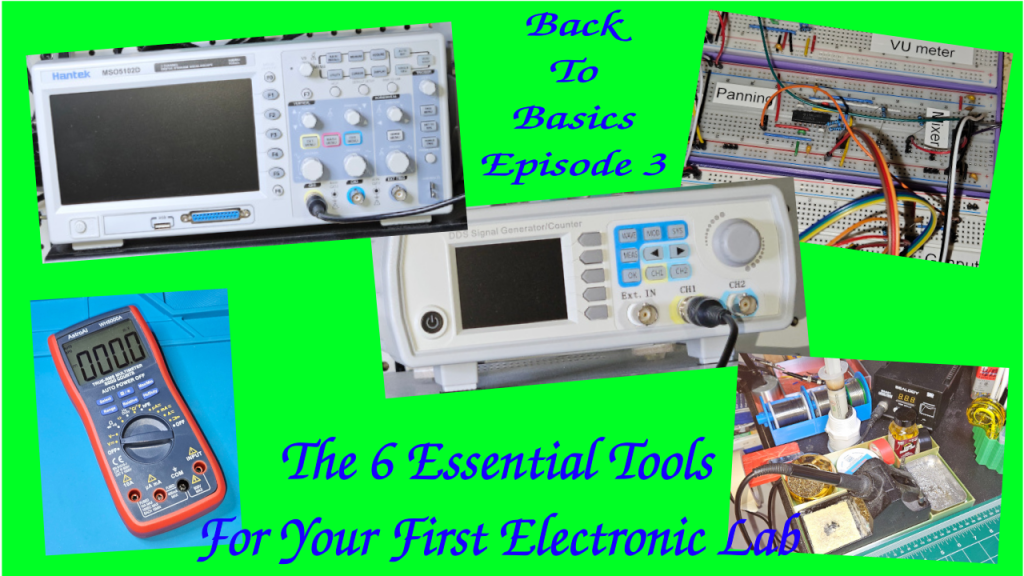
Today, we’re building your first electronics workbench. We’re going to break down the six most essential pieces of gear—from the absolute must-haves to the powerful diagnostic equipment you’ll eventually crave.

I’m structuring this into three simple tiers, to make it progressive.

Tier 1: The Must-Haves, which are the stuff you need on Day 1 to even build a circuit.

Tier 2: The Essential Builder Stuff or how to make your project permanent.

Tier 3: The Diagnostic Duo or how to troubleshoot and see signals you can’t see with your eyes. That’s for when you need to actually see the electricity doing its thing.

Let’s start building!


Tier 1 – The Absolute Must Have: The Prototyping Pair

Let’s dive into tier one. The prototyping pair. First up, the breadboard, your best friend for starting out. It’s basically a temporary solder-less lab.

It will let you try things out, make mistakes, swap components. Basically: super fast iteration.

The key thing to get, though, is how it’s wired internally. Those middle columns, they connect vertically. Little strips of metal inside. You plug your component legs into different rows in the same column, and they’re connected.

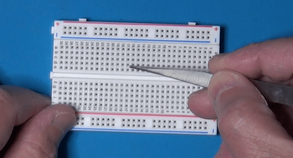
Those long strips on the sides, the power rails, run horizontally all the way from left to right. Knowing that difference saves hours of confusion. So vertical columns for components in the middle, horizontal rows for power on the sides. Simple when you know it.

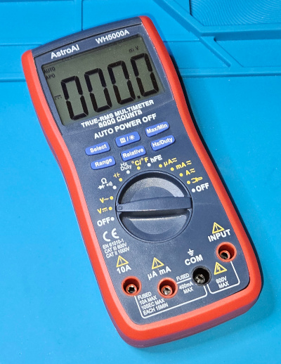
Once you’ve built something, you need to check if it actually works or why it doesn’t. Which brings us to the second must-have in Tier 1, the digital multimeter, or DMM. The Swiss Army Knife. You just can’t debug what you can’t measure. It’s fundamental. Safety, too. Measures voltage, current, resistance, the basics.


Tier 2 – The Essential Builder: Permanent Connections

Let’s now move on to Tier 2, the essential builder.

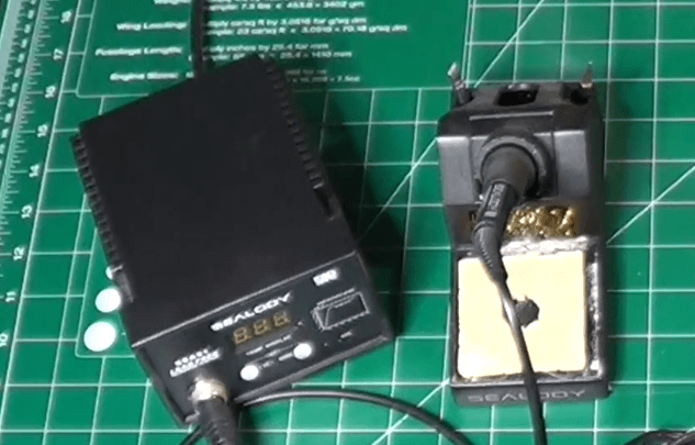
So your breadboard circuit works perfectly. Awesome. But now you want to make it permanent. Put it on a proper PCB or maybe a perf board. And that means soldering. You need a soldering iron and you need solder. This is where things get hands on. But what iron to use? There’s so many types.

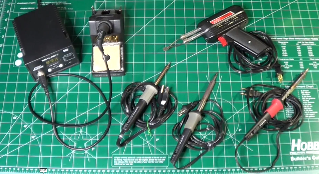
The key thing is temperature control. You need to be able to set the right temperature for your soldering components. Too cold, and you obtain bad joints. Too hot, and you damage the components.

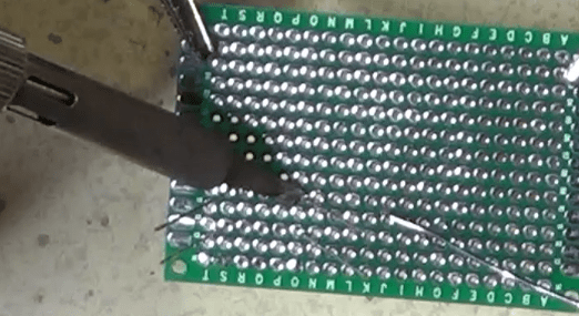
And then you need the proper technique. This is where people often mess up, big time. The absolute number one rule is: melt the solder with the components to attach together, not with the solder tip. You touch the hot iron tip to both the component leg and the copper pad on the board at the same time. You hold it there for a couple of seconds, just long enough for them both to get hot. Then you touch the solder wire to the joint, not to the iron tip. And the heat from the pad and the leg melts the solder, making it flow nicely around them. You’re aiming for that classic shiny volcano shape, a little cone. Not a dull blob. Definitely not a dull blob. Dull or lumpy means a cold joint, which will probably fail later.

Also, always use a fan or work in a well-ventilated area. Those fumes aren’t good for you.


Tier 3 – The Diagnostic Duo: Seeing The Unseen

Now tier three, the diagnostic duo. This sounds more serious. Well, it is, in a way. This is for when you move beyond simple DC circuits into things that change over time, like audio signals or digital clocks.

First in the list is the function generator, or the signal injector. Its job is basically to create predictable electrical signals.

Known, clean waveforms, usually sine waves for analog stuff, square waves for digital, maybe triangle waves for ramps. Why is that necessary? Can’t you just use the signal from, say, the phone’s headphone jack? You could, but is that signal perfectly clean? Does it have noise? Is its amplitude exactly what you think? A function generator gives you a reliable, known-good input. So you’re eliminating unknown variables.

If you test a filter circuit with a perfect sine wave from the generator and the output looks wrong… Then you know the problem is in your circuit, not just some garbage coming in. It’s about controlled testing.

And now the function generator partner, the oscilloscope. The big gun. This is arguably the most powerful debugging tool in electronics. It lets you see electricity.

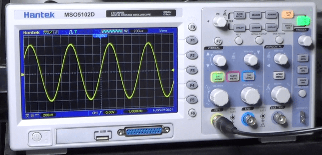
It draws a graph. Voltage on the vertical axis, time on the horizontal. So you can see exactly how a signal changes, millisecond by millisecond or even faster. So you can see noise, distortion, timing glitches. Things way too fast for a DMM.

And the key to using it effectively, the thing that unlocks its power, is the trigger control. It just tells the scope when to start drawing the waveform on the screen.

It looks for a specific voltage level on the signal. So every time the signal hits, say, one volt while rising, the scope starts drawing from that exact point. And because it starts drawing at the same point on the waveform over and over, that fast-moving signal looks like it’s standing perfectly still on the screen. Makes analysis possible.

So you hook the function generator output, like a 1 kHz sine wave, to your circuit input and then probe the output with the oscilloscope. And you can see precisely how your circuit affects that signal, stable and clear, thanks to the trigger. That’s how professionals diagnose high-speed problems.

Conclusion

Let’s recap quickly, by function.

Tier 1, the must-haves for prototyping are the breadboard and the DMM.

Tier 2, the essential builder for making it permanent, is the soldering iron and the solder. And don’t forget the ventilation!

Tier 3, the diagnostic duo for seeing the unseen signals, are the function generator and the oscilloscope.

That’s the core toolkit for your lab.

The really crucial takeaway is that you don’t need everything on day one. It’s scalable.

Start with Tier 1. Get comfortable prototyping. Then, when your projects demand permanence, you move to Tier 2.

And only when you’re dealing with signals where timing and shape really matter, like building an audio filter or maybe something with a micro-controller, you invest in Tier 3 for that deeper diagnostic view.

Start small, build your skills, and let your projects guide how you grow your lab. Build it organically.

You don’t need everything at once!

Finally, here is the link to the companion YouTube Video, which you may want to watch for additional details.

How To Make A PCB Using A Laser Printer

When working with electronic circuits, sooner or later we feel the need to make our own PCBs to get a more functional and better looking circuit board.

I already made a video in the past to show how that could be done, for simple circuits, by drawing the circuit manually on the copper clad with a special kind of pen that uses an ink impervious to the chemicals needed to etch the PCB.

This time, I am presenting you a different technique, that allows you to draw the traces, and also the silk layer, with any of the design tools of your choice available on the Internet and the market in general. All you need to have is a laser printer. You can refer to this newer video for a demonstration of the process.

The whole process works on the concept that the printouts of the laser printers are made with a toner that has the characteristic of being able to protect the copper from the etching chemicals, like the ink from the pen in the original video. This is because the toner is made with a sort of plastic material.

Unfortunately, we cannot use a laser printer to print the masks directly on the copper clad, because the PCB boards are too thick for the printer. Therefore, we need to find a way to print on paper and then tranfer the printed ink to the copper afterwords.

This is made possible by a certain quality of glossy paper that do not allow the toner to stick permanently on its surface when exposed to heat. Even paper from magazines that are printed on glossy paper works relatively well for this to happen. However, there are specialized papers, that are designed specifically for this, which are called Thermal Transfer Paper For PCBs. A quick search on-line will give you plenty of places where you can buy it at a relatively modest price.

Once you have your PCB design ready and printed on such paper, the process to create PCBs becomes really straightforward.

First step is the transfer of the traces drawing to the copper. The copper needs to be perfectly clean, so it is always better to use a piece of steel wool to scrape away copper oxide and other dirt from the copper surface. Just move the wool in a circular fashion to remove all the particles of oxide from the copper clad and make sure to use gloves, otherwise the contact with the skin of your hands will soon oxidize again the copper.

Once all the oxide is removed, you need to deep clean the copper to remove any particle of dust from it. To do so, you can use some alcohol. Once done, let the board stand for a a while to make sure it is completely dry.

Then lay the board on the printout, making sure the copper is in contact with the drawing. Wrap the paper all around the board to make sure it will not move during the transfer process.

Once the PCB is wrapped with the paper, put it on the table copper-side up and use an iron at the max temperature, with no steam, to heat uniformly the whole surface of the paper and the pcb wrapped in it. Be careful not to burn yourself in the process, of course. You do not need to press hardly, the weight of the iron is just enough. Just make sure you keep moving the iron so that the whole surface is heated uniformly. Do that for a while, until the copper clad becomes almost as hot as the iron. Don’t worry about burning the paper. it is not going to happen. Paper burns at 451 F while the iron, even at the hottest temperature, doesn’t normally go over 400F.

Once the paper and the clad are well heated, put aside the iron and unwrap the board, making sure that when you remove the paper from the copper side you do that slowly and uniformly. The ink from the printout will now have moved from the paper to the copper.

Second step is the actual etching. Use a plastic container, fill it with some ferric chloride solution, enough to cover the whole pcb, then dump the board in the solution. Once the board is in the solution, you’ll notice that the ferric chloride starts changing color. From the initial brown color, it starts becoming darker and darker. This happens because of the copper on the board that starts dissolving in the solution.

While the etching process continues, try to agitate the solution periodically, which will speed up the reaction. A warmer room will also help. Every now and then, check the status of the board and remove it from the solution as soon as you don’t see any more copper on the surface of it.

Once the etching is completed, remove the PCB from the solution and start rinsing it immediately, to stop the reaction that would continue to attack the remaining copper on the surface.

You now need to remove the toner film from the copper traces, otherwise you will not be able to solder the components on it. To do so, use a Lacquer thinner on a piece f paper or cotton and work slowly a little bit at a time. Do this in a well ventilated area. Solvent vapors are both unpleasant to breath and harmful.

Third step is to drill the holes. It is only necessary if you use pass through components, of course. If you use surface mounted components, this step is not necessary, unless you need holes to hold in place the board.

Finally, the fourth and last step is to do another transfer, on the components side of the board, to transfer the drawing for the silk layer. The procedure is exactly the same, but this time the toner will be lay down directly on the board support, not on the copper.

You can see how this process allows you to quickly repeat the whole procedure on as many boards as you like. You just need to print multiple copies of the layouts on the thermal paper and go through the previous four steps.

Hope yo liked this procedure, and don’t forget to go watch the corresponding video, so you will see exactly how this procedure works.

More on the Theremin: The Heterodyne Mixer

The heterodyne mixer is the stage of the Theremin where the high frequency signals coming from the pitch reference oscillator and the pitch variable oscillator are combined together to obtain the audio signal.

mixer

Here we are again with another post about the Theremin, which can be considered the first electronic musical instrument ever invented, almost 100 years ago, in 1919, by the Russian physicist Leon Theremin.

At that time the Theremin was made out of thermionic valves and used a lot of space and electric power.

theremin_in_concert

Today, thanks to the evolution of electronics in the last century, we can make one that can occupy much less space while also consuming much less power. In fact, this is one of several articles that I have already published on the design and construction of such musical instruments, using solid state components.

Please consult this site archives for the previous articles on the subject and THIS link for schematics and diagrams, which I keep updating as I go in designing and building the pieces of the instrument

A corresponding series on the Theremin is also available on YouTube at THIS link. There, I describe every detail of my project, explaining how the various parts of the device work and how I built everything so far in a very inexpensive way.

In this article I will explore the Mixer stage of the Theremin, describing how it works and how it is used within the Theremin itself.

The mixer is the Theremin stage that combines together the signals from the pitch variable oscillator and the pitch reference oscillator, to create an audio signal that is essentially the sound that the Theremin produces.

The combination of the two input signals is done with a process called heterodyne. It basically consists in multiplying the two input signals by exploiting the non-linear characteristic of transistor Q1, which is carefully polarized outside its linear zone. The result of the multiplication is a new complex signal containing frequencies that are the sum and the difference of the frequencies of the original input signals. Since the frequencies of those input signals are close to each other, their difference falls in the audible range, which is what produces the peculiar sound of the instrument.

Looking at the schematic, you can see that the two input signals are mixed together at the base of transistor Q1, which they reach passing through capacitors C4 and C8, used to decouple the mixer from the direct current superimposed to the input signals.

Transistor Q1 is polarized in the non-linear zone of its characteristics. Because of the non-linearity of the transistor, the two signals end up being multiplied with each other, producing a new, more complex, signal that contains both the sum and the difference of the frequencies of the input signals. This heterodyne process, therefore, applies the following equation to the two input signals:

sin(2πf1t) * sin(2πf2t) = 1/2 cos(2πf1t – 2πf2t) – 1/2 cos(2πf1t + 2πf2t)

where the factors on the left side represent the two sinusoidal input signals, and the resulting complex signal is on the right side of the equation. The above formula is actually a simplification, because it does not take into account the phase shift between the two input signals, which should appear as a phase factor in the parameters of each of the sine waves on the left side of the equation. However, if we did the full calculations, we would see that we would still obtain the same output waves, but each would have an extra amplitude factor that depends on the initial amplitude of the input signals and on their phase shifts.

Anyway, the complex signal obtained at the collector of transistor Q1 is supplied to a Low Pass filter, made up of the components R4, R7, R8, R9, C2, C3, C5, C6 and C7. The filter produces an attenuation of the high frequency element of the complex signal, effectively leaving only the one at low frequency  cos(2πf1t – 2πf2t), which is the audio signal.

That output signal is then passed to the next stage of the Theremin, the VCA, where it acquires the dynamics of the music sound. We will talk about the VCA in a future post.

If you are interested in more information on the Theremin Mixer and how I built it, please watch this companion VIDEO on YouTube.

And, as always,

Happy experiments !!!