It sometimes happens that we build something out of necessity, to help us with little day-to-day tasks, and this is the case for today’s project.
The boiler’s room in my basement is a very cramped place that I need to access frequently because I keep in there a freezer for groceries. It turns out that I often have my hands full when I come back from taking something from the freezer, and it is difficult to reach for the light switch.
To obviate to this problem, I decided to build an automatic light switch, so I don’t have to maneuver it manually anymore. And, since I was at that, I decided to make one that not just turns off when I leave the room, but also turns on the light automatically when I enter the room.
The core of this device, technically called an Occupancy Sensor, is a PIR, or Passive Infrared sensor. I have a version of it called HC-SR501 that puts together a Pyroelectric Infrared Detector, or PID, with a bunch of other electronic components that make the sensor useable with very few external components. The PID is concealed underneath that white little dome, which is nothing more than a Fresnel lens that concentrates the light on the actual sensor, thus increasing its sensitivity.
The PID used in this device is called LHI 778, and is capable of detecting infrared emissions over a background noise of up to 85 degrees Celsius. You can see from its data sheet that it is like a small metallic cylinder with 4 pins coming out of it. This PID actually contains two infrared sensors connected in series, to increase its sensitivity.
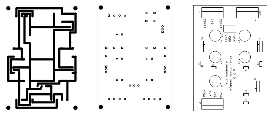
This one is the schematic I made to use the PIR motion detector. The Detector is connected through the pin header J1 on the left. The header provides the power supply for the detector on pins 1 and 3, and captures the output signal on pin 2.
The signal from the detector goes to the base of transistor Q1 which pilots a relay that is used to control the lights of the room where the device is located.
The 5V power supply for the transistor and the relay comes from an old USB charger, so I didn’t have to build a power supply just for this application. LED1 and R1 provide a visual indication that tells us when the gadget is turned on.
The actual power supply for the whole thing comes directly from a 120V socket, goes through a 1A fuse, and through a power switch.
When the switch is set to on, both the USB charger and the common terminal of the relay receive the 120V. Power socket J3 receives the 120V only when the switch is on and, simultaneously, the PIR detects the presence of a person.
The following archive contains all the files you will need if you decided to build this device for yourself, and more.
You can also watch this video for further details on the construction of this device.
Important note: this device involves the use of potentially deadly voltages and you should not try to replicate it if you have no experience with high voltages. Build it at your own risk.
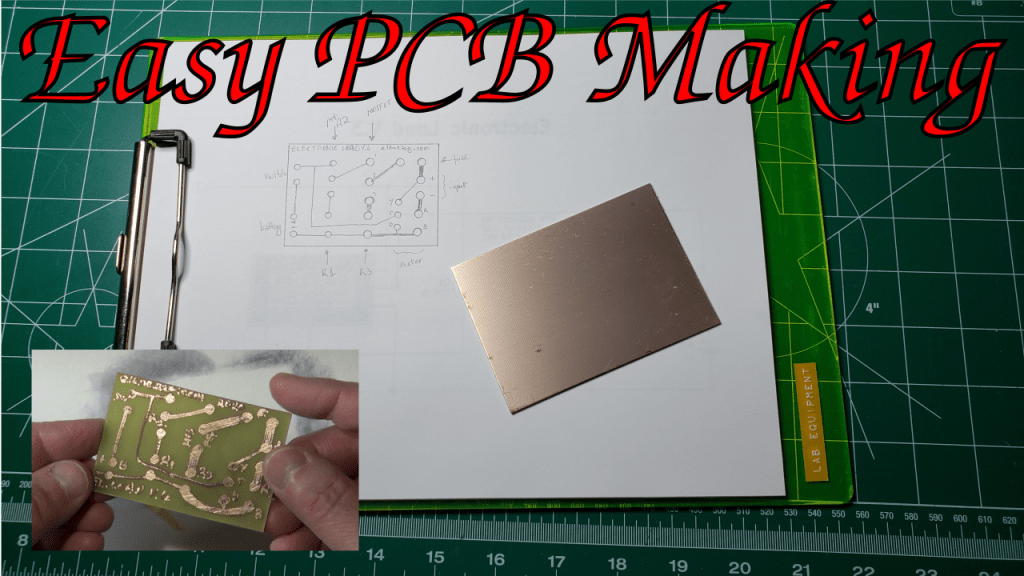
When working with electronic circuits, sooner or later we feel the need to make our own PCBs to get a more functional and better looking circuit board.
I already made a video in the past to show how that could be done, for simple circuits, by drawing the circuit manually on the copper clad with a special kind of pen that uses an ink impervious to the chemicals needed to etch the PCB.
This time, I am presenting you a different technique, that allows you to draw the traces, and also the silk layer, with any of the design tools of your choice available on the Internet and the market in general. All you need to have is a laser printer. You can refer to this newer video for a demonstration of the process.
The whole process works on the concept that the printouts of the laser printers are made with a toner that has the characteristic of being able to protect the copper from the etching chemicals, like the ink from the pen in the original video. This is because the toner is made with a sort of plastic material.
Unfortunately, we cannot use a laser printer to print the masks directly on the copper clad, because the PCB boards are too thick for the printer. Therefore, we need to find a way to print on paper and then tranfer the printed ink to the copper afterwords.
This is made possible by a certain quality of glossy paper that do not allow the toner to stick permanently on its surface when exposed to heat. Even paper from magazines that are printed on glossy paper works relatively well for this to happen. However, there are specialized papers, that are designed specifically for this, which are called Thermal Transfer Paper For PCBs. A quick search on-line will give you plenty of places where you can buy it at a relatively modest price.
Once you have your PCB design ready and printed on such paper, the process to create PCBs becomes really straightforward.
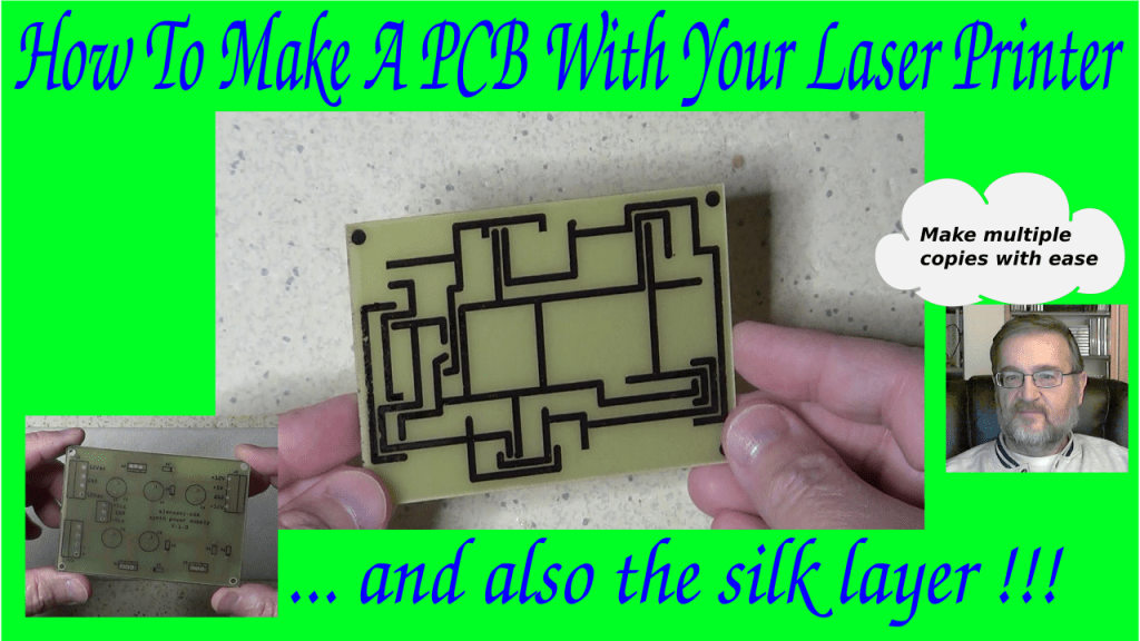
First step is the transfer of the traces drawing to the copper. The copper needs to be perfectly clean, so it is always better to use a piece of steel wool to scrape away copper oxide and other dirt from the copper surface. Just move the wool in a circular fashion to remove all the particles of oxide from the copper clad and make sure to use gloves, otherwise the contact with the skin of your hands will soon oxidize again the copper.
Once all the oxide is removed, you need to deep clean the copper to remove any particle of dust from it. To do so, you can use some alcohol. Once done, let the board stand for a a while to make sure it is completely dry.
Then lay the board on the printout, making sure the copper is in contact with the drawing. Wrap the paper all around the board to make sure it will not move during the transfer process.
Once the PCB is wrapped with the paper, put it on the table copper-side up and use an iron at the max temperature, with no steam, to heat uniformly the whole surface of the paper and the pcb wrapped in it. Be careful not to burn yourself in the process, of course. You do not need to press hardly, the weight of the iron is just enough. Just make sure you keep moving the iron so that the whole surface is heated uniformly. Do that for a while, until the copper clad becomes almost as hot as the iron. Don’t worry about burning the paper. it is not going to happen. Paper burns at 451 F while the iron, even at the hottest temperature, doesn’t normally go over 400F.
Once the paper and the clad are well heated, put aside the iron and unwrap the board, making sure that when you remove the paper from the copper side you do that slowly and uniformly. The ink from the printout will now have moved from the paper to the copper.
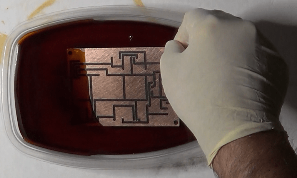
Second step is the actual etching. Use a plastic container, fill it with some ferric chloride solution, enough to cover the whole pcb, then dump the board in the solution. Once the board is in the solution, you’ll notice that the ferric chloride starts changing color. From the initial brown color, it starts becoming darker and darker. This happens because of the copper on the board that starts dissolving in the solution.
While the etching process continues, try to agitate the solution periodically, which will speed up the reaction. A warmer room will also help. Every now and then, check the status of the board and remove it from the solution as soon as you don’t see any more copper on the surface of it.
Once the etching is completed, remove the PCB from the solution and start rinsing it immediately, to stop the reaction that would continue to attack the remaining copper on the surface.
You now need to remove the toner film from the copper traces, otherwise you will not be able to solder the components on it. To do so, use a Lacquer thinner on a piece f paper or cotton and work slowly a little bit at a time. Do this in a well ventilated area. Solvent vapors are both unpleasant to breath and harmful.
Third step is to drill the holes. It is only necessary if you use pass through components, of course. If you use surface mounted components, this step is not necessary, unless you need holes to hold in place the board.
Finally, the fourth and last step is to do another transfer, on the components side of the board, to transfer the drawing for the silk layer. The procedure is exactly the same, but this time the toner will be lay down directly on the board support, not on the copper.
You can see how this process allows you to quickly repeat the whole procedure on as many boards as you like. You just need to print multiple copies of the layouts on the thermal paper and go through the previous four steps.
Hope yo liked this procedure, and don’t forget to go watch the corresponding video, so you will see exactly how this procedure works.
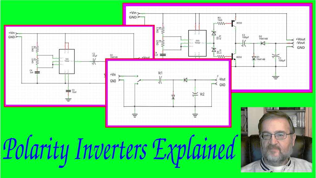
What are polarity inverters and what are used for.
Sometimes we design and build a circuit that needs a dual power supply. But, in certain cases, we really need just a positive voltage to power a circuit and the negative is only used for some special polarization that doesn’t really need the same amount of power used for the positive. Consider, for example, a circuit with a depletion channel MOSFET that requires a negative voltage just for the polarization of its gate.
In such cases, it is economically better to use a different approach than having a full fledged dual power supply. This approach is called “polarity inversion”, resulting in a device that is able to convert the positive voltage of a power supply into a low current negative voltage.
A polarity inverter is, therefore, a circuit that is capable of taking a positive voltage with respect to the ground and generate a negative voltage also with respect to the ground, so that we can have both a positive and a negative voltage available at the same time to power another circuit, without using a dual power supply.
In principle, the inverter is based on the following circuit.
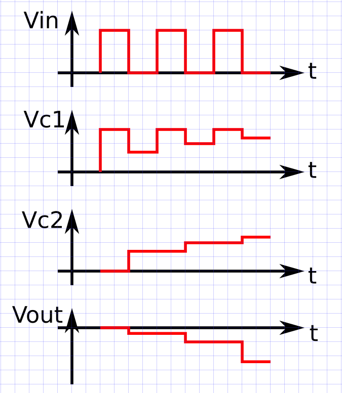
There are two capacitors and two diodes, and a switch that connects the positive of the first capacitor alternatively to the positive voltage source and to the ground.
When the switch is set toward the positive voltage, capacitor C1 starts charging through the first diode, which closes the circuit toward the ground. Given enough time, the voltage at the capacitor increases up to the input voltage minus the voltage drop on the diode.
For example, if the input voltage is 9V, the capacitor will charge to about 8.4V.
This is represented in the following diagram by the first pulse on Vin and the corresponding voltage on C1.
Now, once the capacitor is charged, we move the switch toward ground. Doing so, we open the circuit that connects capacitor C1 to the input voltage and, instead, we connect the same end of the capacitor toward ground.
This way, the voltage at the capacitor C1 is now providing a forward polarization to the second diode, the one on the right, and therefore we have a closed circuit that goes from capacitor C1, to capacitor C2 and through the second diode.
If we choose the two capacitors with the same capacitance, half of the charges on capacitor C1 will transfer to capacitor C2 and, as a result, both capacitors C1 and C2 will end up with half of the original charge and, therefore, with half of the original voltage that was on C1.
This is represented by the second part of the above diagram, where now the input voltage is zero, but capacitors C1 and C2 are at half the original voltage.
On the next cycle, we move the switch back toward the power supply, so capacitor C1 is again charged to the input voltage. In this case, however, the second diode is inversely polarized, so capacitor C2 is isolated and cannot either charge nor discharge, thus it keeps the previous value of voltage.
Moving the switch back to the ground, C1 gives now some more charge to C2 and, therefore, its voltage drops a bit while C2 voltage, instead, increases more.
And you can now see that if I keep switching back and forth, adding more cycles to the diagram, both C1 and C2 keep retaining more and more charges, and their voltage keep increasing so that, after a number of cycles, C2 has reached about the same voltage as the input.
Now, note how capacitor C2 is connected to the ground on its positive side, and the other end is offering its negative voltage to the the output of the circuit that is thus negative with respect to the ground.
If you look at the last of the four diagrams, in fact, you can see how the output voltage becomes more and more negative with respect to the ground, with a tendency to reach the 8.4 V we mentioned before.
So, if we keep moving the switch back and forth quickly, after reach that state we can sustain it, even if we remove a little amount of charge from C2 at each cycle, due to a load that we could put across its leads.
This circuit is called a charge pump, because is able to pump charges into the second capacitor, even if it is not directly connected to the input voltage.
Note that if we start applying a strong load to the output, C2 won’t be able to recharge fast enough and its voltage will start dropping. And that is why we cannot use this polarity inverter for loads comparable to those that we can put directly on the original power supply.
But, how do we move a switch fast enough to obtain this functionality?
The trick is to replace the mechanical switch with a a solid state one, and control it with a square wave oscillator, the so called astable multivibrator.
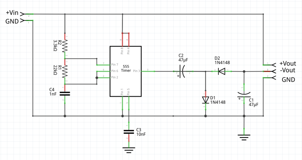
One way to do that is to use a 555 timer, like in the following schematic.
The circuit on the right half side is exactly the same as the one in the previous schematic. However, on the left half side, the mechanical switch has been replaced with a 555 timer setup as an astable multivibrator, with a duty cycle close to 0.5.
Pin 3 of the 555, which is the output pin, will move alternatively from the voltage of the power supply to the ground, thus working as if it was the switch of the previous schematic.
The oscillation frequency is provided by R1, R2 and C4, which I calculated in this example to provide a frequency of about 30 kHz with a duty cycle very close to 0.5.
If you would like to know more about the 555 timer, I suggest you to watch the video I made about one year ago where I describe what it is and how it works. Here is the link to the video.
In order to be able to support relatively higher currents with the polarity inverter, we need to be able to recharge the capacitors at a faster pace, which translates in a higher current. One way do so is by using the output of the 555 to pilot a couple of transistors with a high value of beta, the coefficient that express the amplification in current of the transistors. With a higher available current, the capacitors will charge faster and, therefore, it will be possible to handle a higher load current.
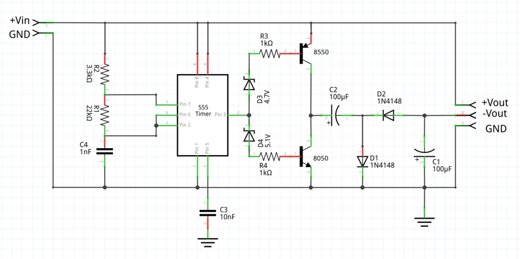
Here is an example circuit that can provide higher currents:
This circuit is basically identical to the previous one but, instead of applying the output voltage of the 555 directly to the charge pump, made of C1, C2, D1, and D2, the 555 controls the two transistors 8050 and 8550, respectively an NPN and a PNP.
With these transistors, we can still connect the positive lead of C2 to the positive of the power supply and to the ground alternatively, and we can force the charges in and out of the two capacitors to move at a faster pace.
The two resistors R3 and R4 are necessary to limit the amount of current through the base of the transistors. Too much current in there would have two unwanted side effects:
First, the transistors could burn because of too much current.
Second, even if the transistors did not burn, they would still go deep into saturation, which would make them spend more time moving between the on and off states and causing the circuit not to work as expected.
In addition to that, since the voltage at the output of the 555 does not change instantaneously between 0 and Vin, there would be a period, during the transition, where both transistors would be on at the same time. As a result, the input voltage would be short circuited for a little while during each cycle, which is a condition definitively to avoid.
To fix the problem, I added those two Zener diodes to the circuit. The Zener diodes create a gap between 4.7V and 5.1V that will prevent the transistors from being both on at the same time, thus fixing the short circuit problem.
Here is how it works.
During the transition from 0 to 9V on pin 3 of the 555, transistor 8550 will be on in the interval between 0 and 4.7V.
During the interval between 4.7V and 5.1V both transistors will be off and, finally, during the transition between 5.1V and 9V, transistor 8050 will be on.
Viceversa, during the transition from 9V to 0, the opposite sequence will happen: first, transistor 8050 will be on, then both transistors will be off, then transistor 8550 will be on, alone.
And that is why the two zener diodes make sure that the two transistors will never be on at the same time, thus protecting them and the power supply.
The final effect will still be the same: the positive lead of C2 will be alternatively connected to the positive and to the ground, making the charge pump to work, and creating the negative output.
To conclude, polarity inverters have their usefulness in certain situations, but are not good enough to replace a full fledged dual power supply.
So, when do we use one or the other?
We will use the polarity inverter in those cases where only a little load is required on that specific pole, whereas the majority of the load would depend on the single power supply.
Whenever we need considerable and comparable amount of power on both the positive and the negative poles, we will need to use a dual power supply.
And finally, if you would like to see the polarity inverter in action, you may want to watch this video, which I posted back in December 2020.