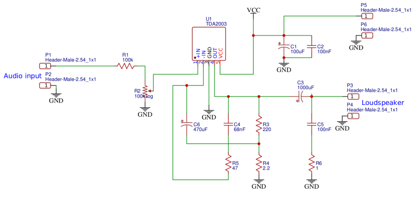
The Theremin v2 audio amplifier and preview audio amplifier share the same schematic.
The input of the amplifier is on pins P1 and P2, where P2 is the ground connection. The input is supposed to be DC decoupled with a small electrolytic capacitor, as suggested by the data sheet of the integrated circuit TDA2003, which is the main component of this amplifier. However, the capacitor was not put in this schematic because it will find its place directly on the output of the audio generator stage. No reason to have two capacitors in series: one at the output of the audio generator and one at the input of the audio amplifier.
The signal coming from P1 goes to a voltage divider consisting of the resistor R1 and the potentiometer R2. When the potentiometer cursor is all the way toward ground, there will be no signal going to pin 1 of the IC and, therefore, the amplifier will be silent. When the potentiometer cursor is all the way toward resistor R1, the signal coming from P1 is divided exactly in half, since the value of the potentiometer R2 and of resistor R1 are exactly the same. This is the position where the volume will be the maximum possible.
I chose the value of 100K for both R1 and R2 so to have a relatively high impedance toward the audio generator, so its output won’t be affected by the movement of the potentiometer. At the same time, I wanted a value of R2 low enough to keep the input of the amplifier solidly on the ground when there is no input signal.
R2 is a logarithmic potentiometer, which means that its value changes according to a logarithmic scale. This is done to compensate for how we perceive the sound volume: the potentiometer increases the power of the sound wave in the opposite way as our ear perceives it. This way, we feel that the volume increases and decreases linearly when we turn the potentiometer.
The output from pin 4 of the IC goes to the loudspeaker through capacitor C3, which is used to prevent that a DC current goes all the way through. In addition, capacitor C5 and R6 provide a high pass filter that shorts to ground all the high frequencies that are not supposed to go to the loudspeaker. Values of capacitors C3 and C5 and the resistor R6 reflect the suggestion on the data sheet.

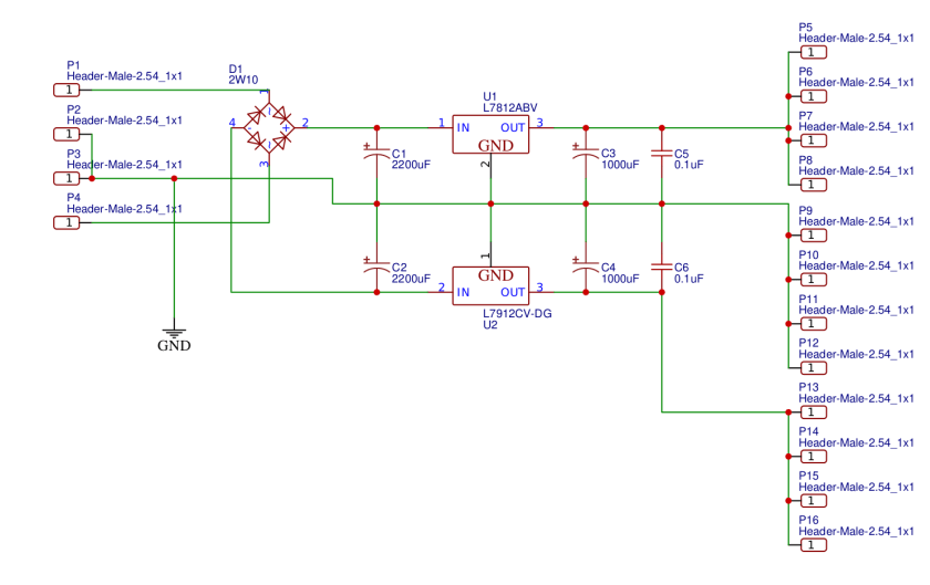
The power supply comes in through pins P5 and P6 and is filtered by capacitors C1 and C2.
C2 takes care of shunting toward ground any unwanted high frequency signal coming from/to the power supply. Capacitor C1, which is a high value electrolytic capacitor, is mostly used to boost the input current when the amplifier requires sudden increases due to peaks of the volume. These capacitors have also the values suggested by the data sheet.
The last part of the amplifier is the negative feedback loop, connected between pins 4 and 2 of the TDA2003. The loop is composed of capacitors C4 and C6, and the resistors R3, R4, and R5.
The negative feedback is used to limit the output power of the amplifier outside the region of frequencies where it is requested, thus preventing auto oscillations of the amplifier, which would otherwise behave like an oscillator.
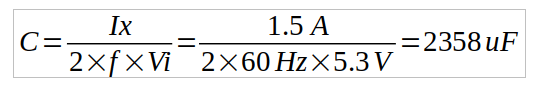
The values of these components are again those suggested by the data sheet. However, C4 and R5, which correspond to Cx and Rx in the data sheet, are calculated based on the data sheet formulas visible in the above picture, where B is the maximum frequency of the signal that we want to amplify, which I set to 10kHz. I don’t believe we want to hear from the Theremin sounds that are above that frequency.
For further information on this amplifier and for a demonstration on how it works, please refer to my corresponding YouTube video.