Behind The Scenes Of The Theremin Design

How I design my electronic circuits and prepare the videos to show them to you.

20180915_153351

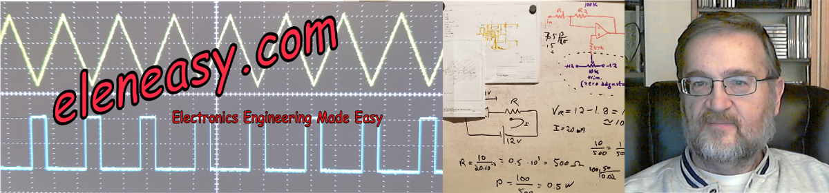
Did you ever ask yourself where I get the schematics of the Theremin circuits and other gadgets that I present on my YouTube videos? The answer is simple: I do some research on books, on specialized magazines and on the Internet. I see solutions created by other people, if any, and then I think about what would better work for my case. Sometimes it ends up to be a modification of something that somebody else did, maybe for a totally different purpose. Sometimes, I just use the general idea to create something different, new, my own design that is more appropriate for my needs.

20181213_105525

Either way, I usually build a number of prototypes of what I need, then I take some measurements in lab, then I start making further modifications to my original design, until I obtain exactly what I am looking for.

20181213_105610

Also, more often than not, I figure that the circuit I am testing is too sensitive to certain parameters of the circuit itself. Maybe is a capacitor which value needs to be adjusted a little bit, or a connection between two or more components that causes issues because of capacitive or inductive coupling with other components. That is when I try to change my design to reduce such sensitivities, so that the circuit can be assembled by anyone with the exact same results as mine. And this is what is called engineerization, or adjusting the design for mass production.

20180915_153412

And sometimes, to do so, it is not enough to test the single circuit. Instead, I need to connect the circuit with other pieces that have to work together with it, and see if further unwanted interactions happen, so that I can eliminate them or, at least, reduce them so that they become negligible.

20180915_153256

Sometimes this process goes fast, sometimes takes a long time. And that’s why my videos are not published at fixed intervals. Unfortunately, since this is done only as a hobby, I don’t always have enough time to dedicate to my project, so days go by until, finally, I am done. Then I finalize my schematics, I build the last prototype and the final product and, in the process, I also record all these activities so I can end up making a video out of them.

20180915_153313

Then the video editing process starts and, once the video is finally ready, I release it on YouTube for you to watch it.

One day I will be able to do this full time. Who knows, maybe when I retire. Or, maybe, if you all give me a hand, this could become my new full time job (donations, donations, donations). We’ll see.

Thank you for reading this article. And, as usual, happy experiments!

Advertisement

DC Electronic Loads

An electronic load to test DC power supply devices up to 100W.

What do you use when you have to test a new power supply that you just built, or one that you bought and want to know if the declared specs are true?

One thing you’ll need is a passive load that you attach to the power supply output to drain a certain amount of current, both to verify that the power supply is capable of providing that amount of current, and to verify the amount of ripple that was not filtered away by the power supply itself.

rheostatA classic method for doing so is to use a rheostat, which is essentially a potentiometer capable of dissipating the amount of power produced by the power supply. The resistance of the rheostat can be changed and therefore different amount of currents can be used to test the power supply. However, rheostats are big, heavy and cumbersome.

An alternative to rheostats is to have a so-called Electronic Load. These are electronic circuits that are capable to emulate the functionality of a rheostat.

I’m proposing here two simple versions of an Electronic Load, functioning in DC, and capable of dissipating up to 100W, all of this in a very condensed space, and very light in weight.

The first version is a very simplistic one.

100W_el_load_v1

It uses a cascade of three transistors, in a configuration called Darlington. This configuration is effectively equivalent to a single transistor with a gain (hfe) that is the product of the gain of all the transistors in the configuration. This allows for a very little control current flowing into the potentiometer used to regulate the base current, and for a high current available between the collector and the emitter of the transistor Q3, in the above schematics.

This circuit does not need its own power supply, since it gets what it needs directly from the power supply under test. The resistor R1 is calculated based on the highest voltage that the circuit will be able to handle, in this case 50V. It is important to note, however, that using this load at lower voltages will prevent the possibility to use the full excursion of the potentiometer, thus limiting the sensitivity of the circuit for the control of the current.

The next circuit eliminates the sensitivity problem by providing it own power supply to control the base current of the Darlington, thus eliminating the dependency from the external power supply voltage.

100W_el_load_v2

In fact, in this case, the base current can be adjusted with the potentiometer RV1, which is polarized through the resistor R1 and the trimpot TR1, which can be adjusted to maximize the useful range of motion of the potentiometer, regardless of the voltage applied at the input terminals. This way the electronic load can have the same sensitivity for any input voltage. A digital Volt/Am-meter, powered by the same internal battery, provides a visualization of the voltage of the system under test and the current being drained from it.

I will soon publish a video on my YouTube channel that shows the Electronic Load I built for myself. Please watch for that video to come out. And, in the mean time, can you think which one of the above schematics I used? Did I use the simple one, because less expensive? O did I sacrifice a few extra bucks to gain more sensitivity on the regulation of the load?

I strongly suggest to subscribe for free to my YouTube channel, and also to click on the bell icon that appears after the subscription is done. This will allow you to automatically receive an e-mail whenever I publish a new video. This way you won’t have to go periodically to my channel to check for new posts.

Happy Experiments!

Experimentation Boards

How to experiment with electronic components to try new things and test your designs

It comes the time where you want to do some experiments to learn how a specific circuit works or to test a new circuit that you are designing.

Fundamentally, there are two options for you:

  1. Use a perforated board where you can solder the components to build the circuit you want to test.
  2. Use a solder-less breadboard, which allows you to build the circuit you need and, later, dismantle it without any damage to the components you used.

There is actually a third possibility, which is to use a PCB, or Printed Circuit Board. However, I will not consider that right now. PCB are normally used in later stage of development, when you are ready to put your design in a more definitive form. Using a PCB board at the early stages of design is not convenient, due to the cost and time needed just to produce the board itself over and over again, until you are satisfied with your design.

Personally, when I am in the first stages of a new design, and I need to try  a new piece of electronic circuit, I prefer to use a solder-less breadboard, which allows me to modify the circuit at will while I test different versions of it.

02_DSC00020

Once I am satisfied with the design and I need to build my first real prototype, I then use a perforated board. In this case I lay down all the components on one side of it, normally the one with no metallic pads, and then I solder the components on the other side, where the metallic pads are located. At the same time I start running the cables from the lead of one component to another, to make all the electric connections between components.

02_DSC00027

If what I need is just one circuit for personal purposes, then I might as well end it right there, leaving the circuit on the perforated board. But if I needed to build several of those circuits, then I start thinking of manufacturing a PCB. But this is a subject for another time.

Since I work a lot with Arduino and Raspberry Pi boards, I have also created my own version of experimentation board, which is basically a piece of cardboard that I covered with blue tape, with  a bunch of stuff glued to it: a couple of breadboards, an Arduino Uno, a Raspberry Pi, and a small LCD display. I also added a few little trays to temporarily place some components needed to build the circuit, or to hold bigger components that are part of the project and cannot fit on the breadboards.

02_DSC00023

This configuration allows me to build my experimentation circuits in a neat way, without having too many things lying around on the workbench. It is very easy to move around the built circuit when it is done on such a custom board.

(Watch the video on YouTube: https://www.youtube.com/watch?v=Wv7kVVZvULA&t=13s)

%d bloggers like this: