A Multiple Power Supply For The Workbench


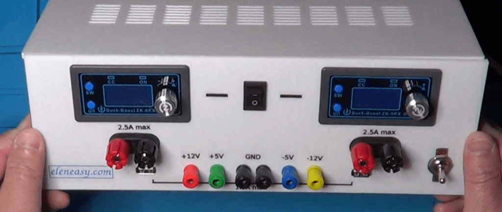
When working with a new prototype on my bench-top, I tend to use one single power supply to power it up. However, sometimes, I need to power up more circuits at once, possibly using different voltages. And it is in those cases that I am forced to use more than one power supply. There are also some cases where I need a dual power supply and, besides the case where I need a +/- 12V, I don’t have a power supply unit capable of giving me other dual voltage values. I even built a simple device, capable of converting a single dual power into a dual one, for those cases where I need it. But that converter is able to provide only a very small amount of power and that is not good when the powers involved are high.


At the end, I need a power supply unit capable of providing me with different voltages at the same time, possibly also current generators and, certainly, the possibility of having both single and dual power supply.
Units on the market capable of providing such features are very expensive, and they don’t even provide all the possible capabilities that I need while, instead, they provide other capabilities that I normally do not care about
To solve this problem, I decided to make my own power supply unit, capable of doing all the things that I find useful in my lab, and at a fraction of the cost of a professional power supply unit.
Let’s take a look at the schematic I designed.


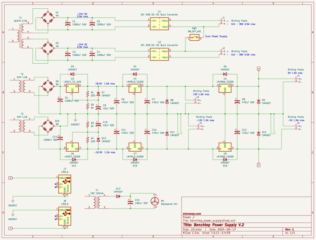
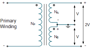
First, in order to be able to connect together a positive and a negative polarity, without having a short circuit, I needed to have totally separated circuits, with independent transformers, so that I could establish any point of reference on each transformer and connect together such points to obtain dual power supplies.
Because of that, I have a total of four transformers in this schematic.
The first on the top, though a single transformer, it provides two independent outputs on two independent secondaries. I used that transformer as the base for building two independent variable power supplies that could be connected together through a switch to obtain a single variable dual power supply, with the two branches independently regulated, useful in certain situations.
The next two transformers, which have exactly the same characteristics, are used to power up the two sides of a fixed dual power supply. One transformer is used for the positive output with respect to the reference point, and the other transformer is used for the negative output with respect to the reference point.
The fourth and last transformer, on the bottom left, is a very small one used solely to provide the power to move a cooling fan for the power supply case.
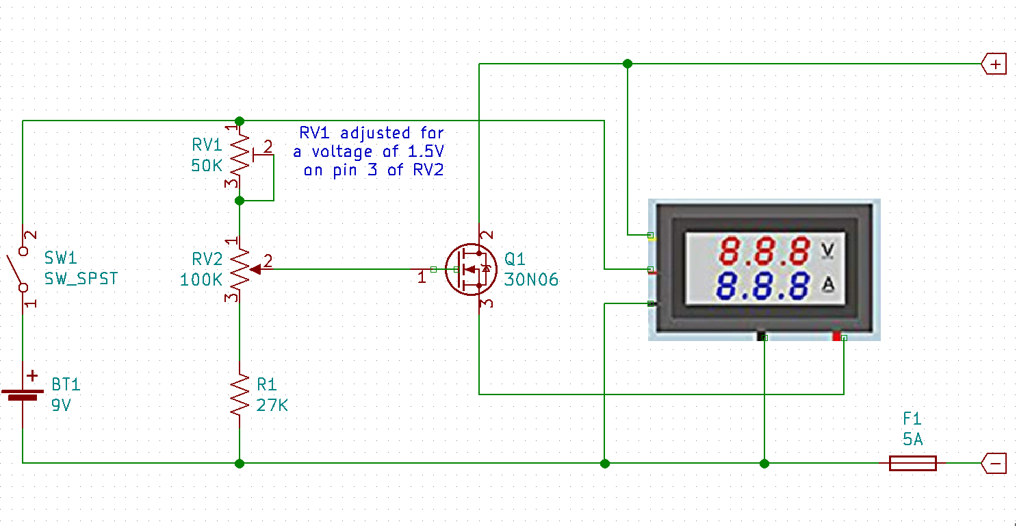
The two variable power supplies are each made around a buck/boost converter manually controllable, which works both as voltage and current generator and also provides a display to visualize various parameters.


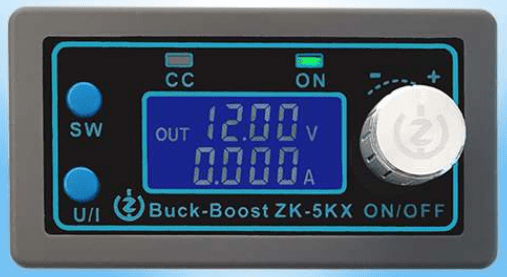
Here is the user manual of this little device.

It has several types of protection, it can be powered with a voltage anywhere in between 6 and 36V, and it can provide a voltage output between 0.6 and 36V, with a maximum current of 5A which can also be regulated, therefore offering the capability of working as a current generator.

It is also very easy to setup and use. It has a 4 wires connector. Two wires provide the input DC voltage and two wires provide the regulated output, either as voltage or current generator.

The manual goes on explaining how to use the rotary encoder and the two auxiliary buttons on the front panel, as well as the dimensions necessary to accommodate the devices on a larger panel of a bigger device.

Going back to our schematic, you can see that I used two of those regulators, represented here with the two blocks. So, each secondary of the large transformer is independently rectified and filtered by this section, to obtain a DC voltage of 34V with up to 2.5A. This two DC voltages go to the input of the power regulators and the outputs are available at the corresponding binding posts on the power supply front panel. Note also the switch that connects together the negative pole of the upper regulator with the positive pole of the lower regulator, to eventually provide a dual power supply where each branch can have and independent value of voltage or current.

The second section, with the two smaller transformers, is the one that provides the fixed voltage power supplies, very useful when working with devices like op-amps, for example, or any other device that needs to be fed with a dual power supply.

The secondary of both transformers T2 and T3 go each through a bridge rectifier and a filtering electrolytic capacitor.

From there, the positive voltage section is made of 3 separate regulators:

– an LM317, which brings down the DC voltage to a more comfortable value for the next regulators

– an LM7812, that provides a +12V to a corresponding output binding post.

– an LM7805, that provides a +5V to yet another output binding post.

Each of the 3 regulators has its own filtering capacitor, to minimize the residual ripple present to the voltage because of the rectification of the AC power provided by the transformer.

You can also see a number of diodes 1N4007, used as a protection for the solid state regulators during the power down of the whole power supply device.

The negative voltage section works exactly the same way, but uses the negative voltage regulators LM337, LM7912, and LM7905.

Another useful feature of this power supply system is the availability of two USB connectors on the front panel, used essentially to provide a 5V power supply, to power USB based devices, or to simply charge the battery of a device that has a USB power connector.

These two USB outlets are visible at the bottom left of the schematic, and it is perfectly visible that only pins 1 and 4 are used, which are those providing the 5V. The data pins 2 and 3 are not even connected.

Finally, the schematic shows also the last transformer, with its own half-wave rectifier and filtering capacitor that powers the cooling fan for the entire case. Why not, since I had laying around that little transformer for which I don’t have any other use.

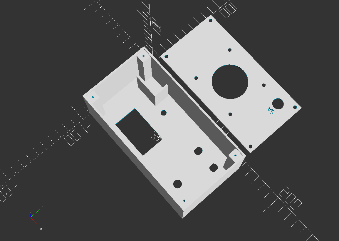
And now, if you are interested in making your own power supply system, I suggest you to take a look at the video presented below, where you can found details on how to make also your own case for the device, as well as a number of useful information for its assembly.

Theremin v.2 Power Supply Design

theremin-v2-power-supply

For the new version of the Theremin, I have chosen to use a dual 12V power supply. This will have more flexibility because it will allow me to use more sophisticated units, possibly using op-amps.

The circuit is very basic: it uses a dual 14V transformer (not shown in the schematic) capable of providing 1.5A at its output.

A dual transformer is made up as in the following picture.

center-tapped-transformer

Is has a primary winding that is connected to the AC power supply outlet, and a secondary winding with a center tapped wire that is usually put to ground on the low voltage circuit side.

Voltage between either end wire of the secondary and the center tapped wire is usually the same (with the exception of specifically made transformers), which we call V.

The voltage measured between the two end wires of the winding is instead two times V or 2V.

Sometimes, instead of having a single secondary winding, we have two, carrying the exact same voltage. In this case, we can connect together the two closest wires and consider that as the center tapped wire. Then everything works as the first kind of transformer.

transformer-trans64

The AC current of the transformer is converted in to a DC current through the usage of a bridge rectifier and the capacitors C1 and C2.

The bridge rectifier converts the sine wave coming from the transformer into a fully rectified wave.

Full-wave_rectified_sine

Then, the capacitor that follows (in this case C1 and C2) starts charging over the ascending sides of the wave and discharging, partially, over the descending sides of the wave, basically filling the wave in between crests and making it look like more a straight horizontal line with some disturbance in it that we call ripple (the red line in the following picture).

ripple

In general, depending on the use of the power supply, we define a maximum value of the ripple that the circuit can handle.

In our case, we need to make sure that the voltage at the input of the regulators never goes below 14.5V, according to the data sheet, otherwise the regulator will not function properly.

The peak voltage provided by the transformer is its RMS value multiplied by the square root of 2, or:

peak_voltage

The minimum voltage we can have at the input of the regulator is:

regfulator_input_voltage

This is the max value of ripple that we can sustain.

To calculate the capacitor necessary to obtain this ripple, we use the following formula:

capacitance calculation

where f is the frequency of the alternate current which, in the USA, is 60Hz, and Ix is the maximum current that the power supply needs to provide.

So, we would need a capacitance value, for C1 and C2, of 2358uF.

However, the Theremin circuit will really not draw 1.5A from the power supply, so we can stay a little conservative, and use the closest value below the calculated one, which is 2200uF.

At this point we can safely say that the voltage on the output of the regulators will be exactly 12V (positive or negative, depending on the output side).

To further help the regulator, and preventing the current through it to go too close to the 1.5A threshold, where the regulator would not work anymore because the ripple becomes too high, we add to the output of each regulator another electrolytic capacitor, this one with a value at least equal to the capacitance value that we did not put at the input side. Since at the input side we put a capacitance of 2200uF instead of 2358uF, we will need a capacitor of at least 158uF.

However, to stay totally safe, I decided to use a capacitor at least 5 times higher, so I used the value of 1000uF for C3 and C4.

And finally, I added an extra capacitor (C5 and C6) to shunt toward ground any RF frequency that would travel back from the Theremin oscillators toward the power supply. A 0.1uF value is what is suggested by the data sheet of the regulator, so I used just that.

Why did I use this capacitor if there was already a 1000uF in there?

The reason hides in the way the electrolytic capacitors behave. In short, the electrolytic capacitors do not work well at high frequencies, so we need to add the extra 0.1uF capacitor, which is not an electrolytic one, to work in that range of frequencies. And since the range of frequencies is much higher than the one of the 110Vac outlet, a very small capacitance is enough to do the job.


DC Electronic Load V.3

Back in August 2018, I presented a DC electronic load on my YouTube channel (V.2). For that, I used an old 2N3055 transistor in a Darlington configuration with 2 more transistors to be able to get enough gain to use it.

100W_el_load_v2

Although declared useful for 100W, I was never able to make it work at those powers due to the limited dissipation capabilities of the power transistor and the heat sink. The max power dissipation I could have from that device was about 20W.

Today, at the anniversary of that presentation, I have created a new version of of the DC electronic load. This new version is based on a MOSFET that can work alone as a load, adjusting the current only through an appropriate voltage on its gate, avoiding the need of having a Darlington circuit with multiple transistors.

The schematic of this new version of the DC electronic load is based on a single MOSFET capable of driving the necessary current, up to 5A and a voltage divider connected to the battery, providing the appropriate voltage to the gate of the MOSFET.

electronic_load-v.3

In order to make it work correctly, the trim-pot RV1 needs to be tuned to obtain a voltage of 1.5V on pin 3 of the potentiometer that regulates the amount of current flowing through the MOSFET, which provides a better use of the multi-turn potentiometer that regulates the actual value of the current.

A combination of digital voltmeter and am-meter, like in the previous version of the DC load, takes care of providing information about the power supply under test.

The device is powered through a 9V battery and it is connected in such a way that the voltage is measured through the yellow wire of the digital voltmeter, wile the current is measured putting the am-meter in series with the MOSFET, with the thick red wire on the source, and the thick black wire toward the negative connector, through a 5A fuse that is used, mostly, to protect the am-meter itself against currents too high of those it can handle.

I made a new case for this new version of the DC load. The main difference is the location of the heat-sink, which is now located on the back panel rather than the top of the device. The new heat-sink is also attached to the back panel through 4 separators, which allow for a better air flow and cooling of the unit when it is used for long period of times.

Here is an OpenSCAD view of the box and the corresponding code to create it.

v3_box_view

$fa=0.5;
$fs=0.5;

//main section
rotate([180, 0, 0]) translate([0, 10, -2])
{
// front panel
difference()
{
cube([150, 80, 2]);
translate([27.5, 40, -1]) cube([45.8, 27.7, 4]);
translate([52, 20, -1]) cylinder(d=6.2, h=4);
translate([120, 60 , -1]) cylinder(d=9, h=4);
translate([108, 20 , -1]) cylinder(d=9, h=4);
translate([132, 20 , -1]) cylinder(d=9, h=4);
translate([3,3,0.5]) linear_extrude(height=2) text(“eleneasy.com – DC load – 25W max.”, size = 6);
translate([36,18,0.5]) linear_extrude(height=2) text(“off”, size=5);
translate([61,18,0.5]) linear_extrude(height=2) text(“on”, size=5);
translate([109,44,0.5]) linear_extrude(height=2) text(“current”, size=5);
}
translate([102.25, 15, 0]) cube([2, 10, 2]);
translate([126.25, 15, 0]) cube([2, 10, 2]);
translate([111.75, 15, 0]) cube([2, 10, 2]);
translate([135.75, 15, 0]) cube([2, 10, 2]);
translate([12, 20, -36]) cube([27, 2, 35]);
translate([39, 4, -36]) cube([2, 18, 35]);

// left panel
translate([0, 0, -60]) cube([2, 80, 60]);

// right panel
translate([148, 0, -60]) cube([2, 80, 60]);

// bottom panel
translate([0, 0, -60]) cube([150, 2, 60]);

// top panel
translate([0, 78, -60])
{
cube([150, 2, 60]);
}

// screws supports
translate([2, 2, -58]) difference()
{
cube([10, 10, 58]);
translate([5, 5, -1]) cylinder(d=2, h=16);
}
translate([138, 2, -58]) difference()
{
cube([10, 10, 58]);
translate([5, 5, -1]) cylinder(d=2, h=16);
}
translate([2, 68, -58]) difference()
{
cube([10, 10, 58]);
translate([5, 5, -1]) cylinder(d=2, h=16);
}
translate([138, 68, -58]) difference()
{
cube([10, 10, 58]);
translate([5, 5, -1]) cylinder(d=2, h=16);
}
}

// back cover
translate([0, 10, 0]) difference()
{
cube([146, 76, 2]);
translate([5, 5, -1]) cylinder(d=4, h=4);
translate([5, 71, -1]) cylinder(d=4, h=4);
translate([141, 5, -1]) cylinder(d=4, h=4);
translate([141, 71, -1]) cylinder(d=4, h=4);
translate([73, 38, -1]) cylinder(d=40, h=4);
translate([126, 60, -1]) cylinder(d=12.5, h=4);
translate([130.5,51,0.5]) rotate([0, 0, 180]) linear_extrude(height=2) text(“5A”, size=5);
translate([(146-55)/2, (76-50)/2, -1]) cylinder(d=4, h=4);
translate([146-(146-55)/2, (76-50)/2, -1]) cylinder(d=4, h=4);
translate([146-(146-55)/2, 76-(76-50)/2, -1]) cylinder(d=4, h=4);
translate([(146-55)/2, 76-(76-50)/2, -1]) cylinder(d=4, h=4);
}

Assembling the circuit is pretty straightforward, and it is done partially in the air and partially  on a perforated board.

We just need to make sure we provide the cables with the right thickness for the current we need to support.

In my case, I used stranded cables with an 18 gauge. These cables are necessary between the thick am-meter cables, the MOSFET source and drain, and the external connectors.

Every other connection can be made with 22 gauge cables.

And finally, the heat-sink should have a resistance of 0.82 Centigrade degrees per watt or less, to prevent the MOSFET from becoming too hot. Note that this will not save the MOSFET in case you draw a current too high. The product between the current and the voltage as provided by the measurements display must never exceed 25W, and the current should never exceed 5A, or the MOSFET will burn.

The tuning is done by measuring the voltage between the terminal 3 of the potentiometer and the ground, with the circuit on, but not connected to any external power supply. The trim-pot has to be adjusted such that the measured voltage equals 1.5V, which is just below the minimum voltage necessary to make the MOSFET conduct current. This way, when turning on the apparatus with the potentiometer all the way to the counter-clockwise position, there will be no current. Then, moving the potentiometer in the clockwise direction, current will start flowing.

Testing of the unit is done attaching it to a power supply that provides different test voltages while we adjust the current with the multi-turn potentiometer on the DC load unit. Just make sure not to exceed 25W of power at any given time. Doing so could damage the MOSFET itself.

I plan to use this DC load in all my future projects that require a power supply of 25W or less, to test the power supply itself. Besides checking that the power supply works fine, you could also check that the ripple of the output voltage does not exceeds your requirements. That can be done connecting the power supply output to an oscilloscope while the DC load draws the current.

And finally, here are a couple of picture of the finished device.

20190816_112540.jpg

20190816_112614

Happy experiments!