Theremin v.1 Pitch Reference Oscillator Analysis

This is my first post of this kind, which I plan to use to give insights on how an electronic circuit is designed. In the future, I plan to post a similar article for every new circuit I design and present on my YouTube channel.

This way, people who are interested in such details can go to this site to get them, thus sparing all the others that don’t care from watching them on the original video.

Today, to get started with the new series of posts, I will go into the insights of the design of the Pitch Reference Oscillator used in the Theremin version 1.

I decided to use the Pitch Reference Oscillator because all the other Theremin’s oscillators are based on the same principle, although for the variable ones, an antenna is added to the resonant circuit to make its capacitance increase based on the position of the hand on the player with respect to the antenna. In fact, the antenna adds up to 8pF to the resonating tank, based on the position of the hand of the player.

For reference, you can watch any of the YouTube videos on my channel related to oscillators in the Theremin Project playlist.

Here is the link to the playlist:

https://www.youtube.com/watch?v=moT9iAaZU-I&list=PL3SNC7XyKklYZOs48Qfh16nTO4t8edDPU

I began the design of the oscillator starting from the base concept of positive feedback amplifier, which can be represented as follows:

feedback_amp

We have an amplifier with a positive gain, which should be 1 when there is an oscillation, and we have a feedback impedance Zf that takes part of the output signal and brings it back to the input of the amplifier. Zf is supposed to be chosen to obtain a positive feedback at the oscillation frequency.

This basic configuration needs now to be modified to insert in it an LC resonating tank. This should be on the output of the amplifier, so its oscillations can be fed back to the input and be sustained with no decay.

oscillator_block_diagram

The amplifier can now be replaced with a real circuit made with a transistor. I choose in this case a common base configuration, which gives me the required gain of almost 1, which is enough to sustain the oscillation.

The Zf will need to provide a phase shift of 90° to compensate for the internal capacitance of the transistor, which will add another 90° for a total of 180°, thus providing a positive feedback, considering that the transistor has actually a negative value of amplification (-1).

Therefore, Zf can be replaced with a simple capacitor that will bring the output signal back to the input with the desired 90° phase shift.

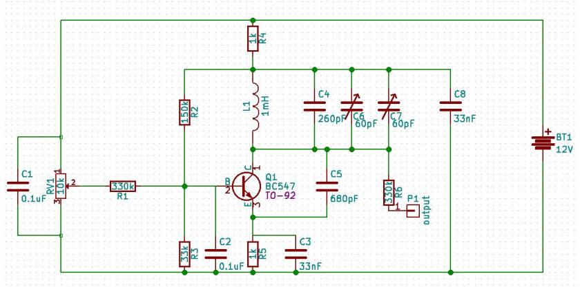
And once all the polarization resistors are added, the circuit looks like the following:

oscillator

In this circuit, R2, R3, R4 and R5 are the polarization resistors, which are calculated based on the specs of the transistor itself.

L1, C4, C6, C7 constitute the resonating tank. The Two variable capacitors are added to allow for a fine tune of the frequency.

C5 is the feedback impedance, or Zf.

The resonating frequency is calculated based on the following formula:

resonating_frequency

where L = L1, and C = C4//C6//C7//CBE = C4 + C6 + C7 + CBE

and CBE is the capacitance between emitter and base.

Temporarily excluding CBE from the calculations, the frequency therefore can vary between 258.2 kHz and 312 kHz. The CBE can be obtained from the transistor data sheet, adjusting for the polarization between base and emitter.

Also, we can slightly affect the resonating frequency of the oscillator by changing the polarization point of the transistor. This can be achieved by a potentiometer added on the base of the transistor itself, as per the following schematic.

final schematic

All the other capacitors in the schematic are used to make the polarization point of the transistor independent from the oscillation frequency, by shunting the oscillation signal toward ground. Thus, their value is such that they behave like conductors with respect to the high frequency of the oscillator.

At the end, considering the increase in capacity given by CBE, the frequency ends up to be centered around 400kHz, which was the required frequency for the pitch reference oscillator.

DC Electronic Load V.3

Back in August 2018, I presented a DC electronic load on my YouTube channel (V.2). For that, I used an old 2N3055 transistor in a Darlington configuration with 2 more transistors to be able to get enough gain to use it.

100W_el_load_v2

Although declared useful for 100W, I was never able to make it work at those powers due to the limited dissipation capabilities of the power transistor and the heat sink. The max power dissipation I could have from that device was about 20W.

Today, at the anniversary of that presentation, I have created a new version of of the DC electronic load. This new version is based on a MOSFET that can work alone as a load, adjusting the current only through an appropriate voltage on its gate, avoiding the need of having a Darlington circuit with multiple transistors.

The schematic of this new version of the DC electronic load is based on a single MOSFET capable of driving the necessary current, up to 5A and a voltage divider connected to the battery, providing the appropriate voltage to the gate of the MOSFET.

electronic_load-v.3

In order to make it work correctly, the trim-pot RV1 needs to be tuned to obtain a voltage of 1.5V on pin 3 of the potentiometer that regulates the amount of current flowing through the MOSFET, which provides a better use of the multi-turn potentiometer that regulates the actual value of the current.

A combination of digital voltmeter and am-meter, like in the previous version of the DC load, takes care of providing information about the power supply under test.

The device is powered through a 9V battery and it is connected in such a way that the voltage is measured through the yellow wire of the digital voltmeter, wile the current is measured putting the am-meter in series with the MOSFET, with the thick red wire on the source, and the thick black wire toward the negative connector, through a 5A fuse that is used, mostly, to protect the am-meter itself against currents too high of those it can handle.

I made a new case for this new version of the DC load. The main difference is the location of the heat-sink, which is now located on the back panel rather than the top of the device. The new heat-sink is also attached to the back panel through 4 separators, which allow for a better air flow and cooling of the unit when it is used for long period of times.

Here is an OpenSCAD view of the box and the corresponding code to create it.

v3_box_view

$fa=0.5;
$fs=0.5;

//main section
rotate([180, 0, 0]) translate([0, 10, -2])
{
// front panel
difference()
{
cube([150, 80, 2]);
translate([27.5, 40, -1]) cube([45.8, 27.7, 4]);
translate([52, 20, -1]) cylinder(d=6.2, h=4);
translate([120, 60 , -1]) cylinder(d=9, h=4);
translate([108, 20 , -1]) cylinder(d=9, h=4);
translate([132, 20 , -1]) cylinder(d=9, h=4);
translate([3,3,0.5]) linear_extrude(height=2) text(“eleneasy.com – DC load – 25W max.”, size = 6);
translate([36,18,0.5]) linear_extrude(height=2) text(“off”, size=5);
translate([61,18,0.5]) linear_extrude(height=2) text(“on”, size=5);
translate([109,44,0.5]) linear_extrude(height=2) text(“current”, size=5);
}
translate([102.25, 15, 0]) cube([2, 10, 2]);
translate([126.25, 15, 0]) cube([2, 10, 2]);
translate([111.75, 15, 0]) cube([2, 10, 2]);
translate([135.75, 15, 0]) cube([2, 10, 2]);
translate([12, 20, -36]) cube([27, 2, 35]);
translate([39, 4, -36]) cube([2, 18, 35]);

// left panel
translate([0, 0, -60]) cube([2, 80, 60]);

// right panel
translate([148, 0, -60]) cube([2, 80, 60]);

// bottom panel
translate([0, 0, -60]) cube([150, 2, 60]);

// top panel
translate([0, 78, -60])
{
cube([150, 2, 60]);
}

// screws supports
translate([2, 2, -58]) difference()
{
cube([10, 10, 58]);
translate([5, 5, -1]) cylinder(d=2, h=16);
}
translate([138, 2, -58]) difference()
{
cube([10, 10, 58]);
translate([5, 5, -1]) cylinder(d=2, h=16);
}
translate([2, 68, -58]) difference()
{
cube([10, 10, 58]);
translate([5, 5, -1]) cylinder(d=2, h=16);
}
translate([138, 68, -58]) difference()
{
cube([10, 10, 58]);
translate([5, 5, -1]) cylinder(d=2, h=16);
}
}

// back cover
translate([0, 10, 0]) difference()
{
cube([146, 76, 2]);
translate([5, 5, -1]) cylinder(d=4, h=4);
translate([5, 71, -1]) cylinder(d=4, h=4);
translate([141, 5, -1]) cylinder(d=4, h=4);
translate([141, 71, -1]) cylinder(d=4, h=4);
translate([73, 38, -1]) cylinder(d=40, h=4);
translate([126, 60, -1]) cylinder(d=12.5, h=4);
translate([130.5,51,0.5]) rotate([0, 0, 180]) linear_extrude(height=2) text(“5A”, size=5);
translate([(146-55)/2, (76-50)/2, -1]) cylinder(d=4, h=4);
translate([146-(146-55)/2, (76-50)/2, -1]) cylinder(d=4, h=4);
translate([146-(146-55)/2, 76-(76-50)/2, -1]) cylinder(d=4, h=4);
translate([(146-55)/2, 76-(76-50)/2, -1]) cylinder(d=4, h=4);
}

Assembling the circuit is pretty straightforward, and it is done partially in the air and partially  on a perforated board.

We just need to make sure we provide the cables with the right thickness for the current we need to support.

In my case, I used stranded cables with an 18 gauge. These cables are necessary between the thick am-meter cables, the MOSFET source and drain, and the external connectors.

Every other connection can be made with 22 gauge cables.

And finally, the heat-sink should have a resistance of 0.82 Centigrade degrees per watt or less, to prevent the MOSFET from becoming too hot. Note that this will not save the MOSFET in case you draw a current too high. The product between the current and the voltage as provided by the measurements display must never exceed 25W, and the current should never exceed 5A, or the MOSFET will burn.

The tuning is done by measuring the voltage between the terminal 3 of the potentiometer and the ground, with the circuit on, but not connected to any external power supply. The trim-pot has to be adjusted such that the measured voltage equals 1.5V, which is just below the minimum voltage necessary to make the MOSFET conduct current. This way, when turning on the apparatus with the potentiometer all the way to the counter-clockwise position, there will be no current. Then, moving the potentiometer in the clockwise direction, current will start flowing.

Testing of the unit is done attaching it to a power supply that provides different test voltages while we adjust the current with the multi-turn potentiometer on the DC load unit. Just make sure not to exceed 25W of power at any given time. Doing so could damage the MOSFET itself.

I plan to use this DC load in all my future projects that require a power supply of 25W or less, to test the power supply itself. Besides checking that the power supply works fine, you could also check that the ripple of the output voltage does not exceeds your requirements. That can be done connecting the power supply output to an oscilloscope while the DC load draws the current.

And finally, here are a couple of picture of the finished device.

20190816_112540.jpg

20190816_112614

Happy experiments!


Conductors, Insulators, and Semiconductors

cpu-3061923_1280

Everybody knows that an electric wire, usually made of copper, is a conductor. And everybody knows that all metals are conductors.

copper-72062_1280

Everybody also knows that plastic is a good electrical insulator, as well as other materials such as glass and rubber.

insulators-3838730_1280

But how about semiconductors? What are they? And how do we really distinguish among conductors, semiconductors and insulators?

To answer all these question we need to look deeper inside the materials.We know that matter is made of atoms, and atoms are made of protons, neutrons and electrons. Protons and neutrons reside at the center of the atom structure, called the nucleus. Electrons are allocated all around the nucleus, at a long distance from it, relatively to the scale of the nucleus itself.

Electrons have a certain amount of energy, that is always an integral value of a certain amount that is called quantum of energy. Depending on the amount of energy they posses, they are locate closer or farther away from the nucleus. The more energy, the farther they are.

Based on quantum mechanics, which we are not going to talk in details in this context, electrons occupy bands of energy. The farther bands in the atom are the so called Valence Band and Conduction Band.

The valence band contains all those electrons that allow the atoms to stick together and forming molecules by bonding with other atoms of the same or a different substance.

water-40708_1280

For certain materials, rather than having molecules, the atoms form what is called a crystalline lattice, which is the case we are more interested in this context. It is worth noting that a new theory, highly based on quantum mechanics, is also distinguishing between actual crystalline lattices and material networks. However, for all the scope and purpose of this context, we will make a simplification and name both of them as crystalline lattices.

lattice(This picture, courtesy of Wikipedia)

In certain conditions, electrons in the valence band can jump to a higher level of energy, thus moving in what is called the conduction band. In the conduction band, electrons are no more stuck to their own atoms, but can start moving freely in the lattice that makes up the material. When that happens, we can control their movement by applying an electric field by the means, for example, of a battery. The voltage of the battery, applied to the two ends of the same block of material (for example a wire), produces the electric field inside the material and forces the electrons to move toward the positive electrode of the battery while, in the mean time, the negative electrode of the battery provides electrons to the material, to replace those that have entered the positive electrode of the battery.

Don’t think that electrons move very fast when they do that. Electrons, in fact, move very slowly, but it is the huge amount of them that help creating a measurable current.

Then you would ask: but when I turn the switch on, the light comes out of a lamp instantly. If the electrons move slowly, shouldn’t a lamp emit light only after a while?

lamp-18869_1280

Well, yes and no. In fact, the lamp does not light up immediately. It takes a certain amount of time to do that. But that time is so small that for us the event happens instantly.

Also, when you turn the switch on, the electrons closest to the positive electrode move into it almost immediately, not because they are fast, but because they are so close to it. At the same time, new electrons are fed to the material from the negative electrode. So, at the end, all the electrons in the wire start moving simultaneously inside of it, causing the current to start flowing immediately.

But I am digressing. Let’s go back to our primary subject.

We have talked about electrons in the valence band and the possibility they have to jump to the conduction band and, thus, helping creating a current if we apply a voltage.

But how much energy do the electrons need to jump to the conduction band?

Here it comes the definition of conductors, semiconductors and insulators.

conductors_semiconductors_insulators

In the materials called conductors, the level of energy that the valence electrons need to jump to the conduction band is basically ‘0’. In fact, valence band and conduction band overlap each other and, therefore, some or all the electrons in the valence band are also, already, in the conduction band. This happens mostly with metals, like copper, iron, aluminum, and so forth. Depending on the particular metal, the conduction and valence bands are more or less overlapped. Those material where there is more overlap are those that conduct electricity better. Those material where there is less overlap, are those that are worst to conduct current, although still conductors.

In the materials called insulators, the gap between the valence band and the conduction band is so high that electrons cannot jump from the valence band to the conduction band, and so they cannot generate an electrical current.
Of course, if we apply a voltage high enough, we can still provide them the energy to make the jump. However, in that case, because of the very high voltage, electrons jump from one band to the other in a disruptive way, causing the material to break. Once that happened, the insulator loose its property and it is no good anymore as such.

Finally, in the materials called semiconductors, the valence band and the conduction band are separated, but close together. It is relatively easy for an electron in the valence band to jump to the conduction band if we only heat a little bit the semiconductor, maybe just with our bare hands. The heat provides enough energy to the electrons to jump to the conduction band. However, not many electrons will do so, unless we keep heating the semiconductor. So, at the end, although capable of conducting some current, semiconductors are not good in doing so. Thus the name of their category.

In this article, we have talked about energy bands in materials, and how materials behave based on the position of the two highest energy band levels.

We have said that conductors are those were valence and conduction bands are partially overlapping.

Conversely, insulators are those that have a high gap in between the valence and the conduction bands.

And finally, semiconductors are those somewhat in between. For them, the valence and conduction bands are separated with a gap, but that gap is small enough to allow, under certain conditions, for the electrons to jump from the valence to the conduction band. That’s why they perform poorly both as conductors and insulators. However, we will see later on how semiconductors can be of great advantage for us, as long as they are treated in a certain way. They are those that allow us to build all the wonders of modern electronics.